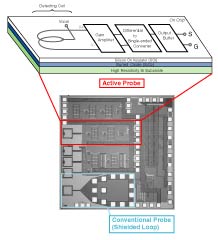
Integrated Active Magnetic Probe
We have developed a novel magnetic probe for the purpose of making a precise EMI* noise map on LSI. In order to achieve both the high sensitivity and the high spatial resolution, a detecting coil and amplifiers are integrated on a single-chip. The active probe has a feature to distinguish the magnetic field from the detected electromagnetic emissions, by means of a differential coil structure and CMOS circuitry techniques.
*Electromagnetic Interference
| 
|
| Implemented active magnetic probe
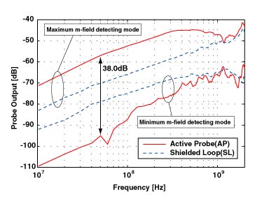
| Measured frequency response of the fabricated probes
|
|
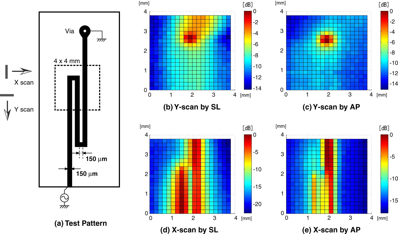
| 2-dimensional magnetic field distribution map
|
References
- S. Aoyama, S. Kawahito, T. Yasui and M. Yamaguchi, "A High-Sensitivity Active Magnetic Probe using CMOS Integrated Circuits Technology", Proc. of IEEE Electrical Performance of Electronic Packaging, pp.103-106, 2005.10.
(The IBM Best Student Paper Award 2005 )
- S. Aoyama, S. Kawahito, and M. Yamaguchi, "Integrated Active Magnetic Probe in SOI-CMOS Technology", Japanese Journal of Applied Physics, Vol.45, No.9A, pp.6878-6833, 2006.09.
- S. Aoyama, S. Kawahito and M. Yamaguchi, "Fully Integrated Active Magnetic Probe for High-definition Near-field Measurement", Proc. of IEEE Electromagnetic Compatibility Symposium, Vol.2, pp.426-429, 2006.08.
- S. Aoyama, S. Kawahito and M. Yamaguchi, "An Active Magnetic Probe Array for the Multiple-point Concurrent Measurement of the Electromagnetic Emissions", IEEE Transactions on Magnetics, Vol. 42, No.10, pp.3303-3305, 2006.10.
[Home] / [Research project]
Copyright(C)1999-2007, Imaging Devices Laboratory
e-mail: webmaster@idl.rie.shizuoka.ac.jp